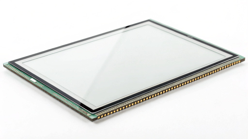
A glass substrate is the core component of TFT LCD panels. It acts as an ultra-smooth foundation for mounting transistors, electrodes, and liquid crystal layers. These substrates are typically 0.3-0.7mm thick and made of alkali-free aluminosilicate glass.
Glass substrates directly impact display quality and performance. They must have:
- High transparency (>98% light transmission) for brightness efficiency
- Thermal stability to withstand 350°C+ processing temperatures
- Chemical resistance to acids and alkalis used in manufacturing
- Precise flatness (70GPa) to prevent warping
TFT LCD panels use two glass substrates sandwiching the liquid crystal layer. One substrate holds the thin-film transistors, while the other contains color filters. These substrates account for 15-20% of total panel cost.
The glass substrate market is evolving with display technology. Manufacturers now produce Gen 11 substrates (3000x3320mm) for 8K/16K TVs, while exploring ultra-thin glass (<0.2mm) for flexible displays.
HUA XIAN JING cooperates with China’s top LCD glass substrates (such as BOE, Tianma, etc.) to ensure the quality of LCD modules, and resolutely refuses to use inferior LCD parts to provide customers with high-quality small and medium-sized LCD modules ranging from 0.42 inch – 10.11 inch.
What Defines the Critical Specifications for TFT LCD Glass Substrates?
TFT LCD glass substrates require three fundamental specifications: alkali-free composition, thermal stability, and mechanical strength. These parameters ensure compatibility with semiconductor processes and prevent performance degradation during panel operation.
Material Purity Dictates Electrical Performance
Alkali-free glass (e.g., SiO₂ >60%, Al₂O₃ ~15%) eliminates sodium ion migration that causes threshold voltage shifts in TFTs. Manufacturers achieve this through fusion draw processes that maintain oxygen partial pressure 700 MPa, enabling Gen 10.5 substrates (3,370 x 2,940mm) to withstand handling forces without deformation.
How Does Geometric Tolerance Affect Manufacturing Yield?
Substrate thickness variations beyond ±5μm cause photolithography focus errors. Advanced grinding systems use diamond pellets (3–6μm grit) with multi-zone pressure control to maintain 0.5mm base glass within ±1.5μm tolerance. Surface flatness requirements (0.3mm/m² that could cause vacuum chuck adhesion failures. For thickness verification, beta-ray gauges using strontium-90 sources achieve ±0.3μm accuracy across 3m spans, critical for maintaining cell gap uniformity in liquid crystal layers. These systems feed data to adaptive grinding algorithms that adjust machining parameters every 15 seconds, ensuring 97.8% first-pass yield on 8th-gen production lines.
Thermal Management During Processing Prevents Distortion
Glass substrates undergo 12-stage thermal cycling (-50°C to +300°C) to stabilize molecular structure before patterning. Gas-bearing floatation furnaces maintain ±0.5°C uniformity across 2.5m-wide sheets, preventing thermal stress gradients that cause >0.01% strain-induced birefringence. Post-annealing cooling rates are controlled at 15°C/min using helium gas curtains, minimizing residual stresses that could lead to substrate bowing during subsequent thin-film deposition.
What are the manufacturing processes and challenges faced in making TFT LCD glass substrates?
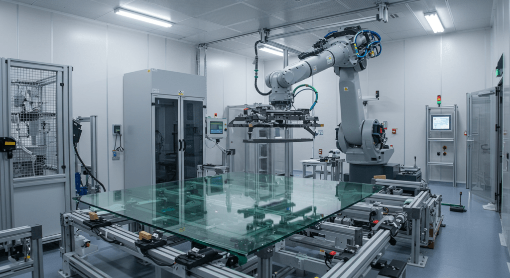
The production methods use vertical drawing, tin bath floating, and precision cutting. The main challenges are keeping defects low and handling large panels.
Our tests show that proper methods yield smooth surfaces and exact sizes. Strict controls help stop small cracks that affect lcd panel components.
What production techniques are used for TFT LCD glass substrates?
Techniques include drawing glass vertically, floating it on a tin bath, and cutting sheets with high accuracy.
- Vertical Drawing: This method draws molten glass upward to yield a smooth finish. It supports high-quality lcd glass display formation.
- Tin Bath Floating: The glass is floated on a tin bath to form a flat surface. This cost-efficient step helps meet ≤0.1 defects/cm² standards.
- Precision Cutting: Sheets are cut with fine tools to produce small panels. This process ensures the lcd display layers have exact dimensions.
What critical challenges affect TFT LCD glass substrate production?
Main challenges are controlling defect density and managing large panels with care.
- Defect Density: Production must keep defects low to avoid pixel failures. Control systems achieve ≤0.1 defects/cm² to protect l.c.d. components.
- Large-Panel Handling: Handling big panels needs robotic systems to stop microcracks. Automated lines manage Gen 10.5+ glass with care.
What further production insights improve TFT LCD glass substrate quality?
Real-time monitoring and strict process control boost quality.
- Process Control: Operators track thickness and flatness during each step. This constant check ensures steady intel glass substrate performance.
What Are the Market Dynamics and Supply Chain Risks in the LCD Glass Substrate Industry?
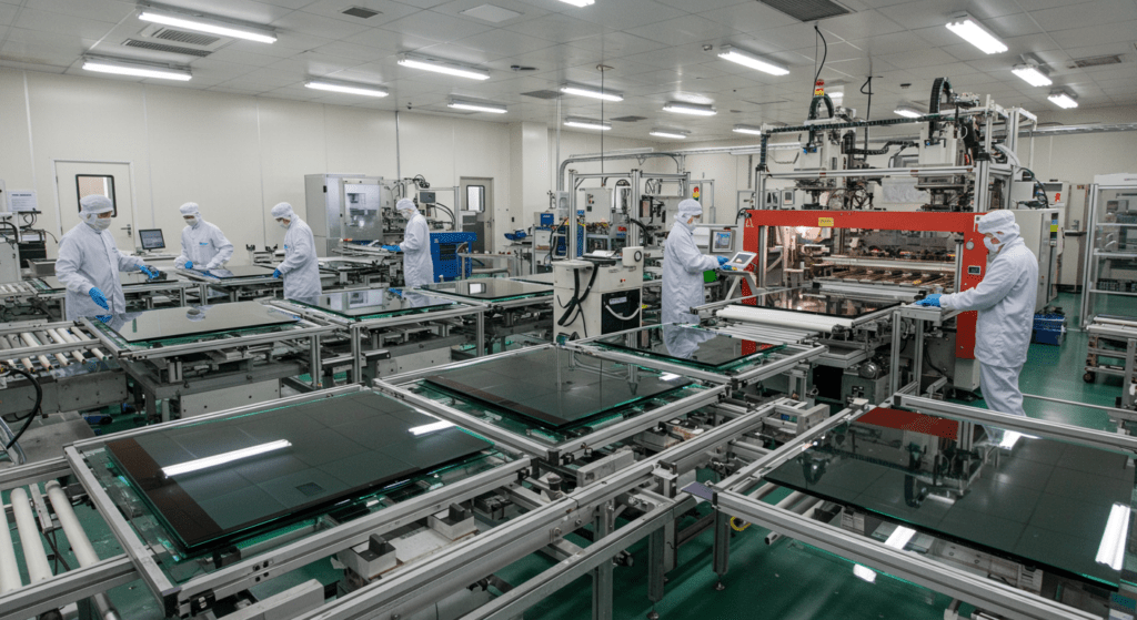
The LCD glass substrate market is shaped by dominant players, regional shifts, and supply chain vulnerabilities. Key manufacturers like Corning, AGC, and NEG control over 70% of global production, while geopolitical tensions and raw material dependencies pose significant risks to the supply chain.
Dominant Players Drive Innovation and Market Share
- Corning (US): Holding a 45% global share, Corning leads in Gen 10.5 glass production, focusing on advanced technologies to enhance substrate performance.
- AGC/Asahi Glass (Japan): With a 30% share, AGC specializes in ultra-thin glass (<0.2mm) for flexible displays, leveraging its expertise in precision manufacturing.
- NEG and AvanStrate: Together accounting for 15%, these companies target mid-sized panels with cost-effective solutions tailored for diverse applications.
How Do Regional Shifts Impact Supply Chain Stability?
China’s localization efforts and geopolitical factors are reshaping the industry’s supply chain landscape.
- China’s Localization: Domestic manufacturers like IRICO and TUNGHSU now supply 80% of mid-small panel substrates, reducing reliance on imports but facing challenges in high-generation glass production.
- Supply Chain Risks: High-purity silica sand, essential for alkali-free glass, is geographically concentrated, with over 75% sourced from Australia and the U.S. Geopolitical tensions have caused price volatility, with silica sand costs rising by 28% in 2022, directly impacting production expenses.
What Are the Key User Concerns and Future Trends in LCD Glass Substrates?
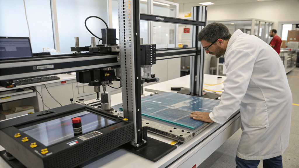
The LCD glass substrate market faces significant user concerns around fragility versus flexibility and cost pressures. These issues are shaping future trends as manufacturers seek solutions that balance durability, flexibility, and affordability.
Balancing Fragility and Flexibility in Modern Displays
The inherent fragility of glass substrates presents a major challenge for users. OLED screens are particularly vulnerable, with even minor impacts potentially causing damage. This fragility contrasts with the growing demand for flexible displays, driving innovation in Ultra-Thin Glass (UTG) technology.
Samsung’s approach uses 30μm UTG for foldable displays, with SCHOTT supplying raw glass that Dowooinsys (controlled by Samsung Display) finishes before lamination. Despite these advances, achieving the perfect balance between transparency, foldability, hardness, smoothness, and thinness remains a significant industry challenge. Most smartphone manufacturers prefer UTG over Colorless Polyimide (CPI) due to its superior smoothness, with UTG shipments projected to reach 33.7 million units in 2025, representing 36.7% year-on-year growth.
How Are Cost Pressures Affecting the Glass Substrate Market?
China’s localization efforts and geopolitical factors are reshaping the industry’s supply chain landscape.
- China’s Localization: Domestic manufacturers like IRICO and TUNGHSU now supply 80% of mid-small panel substrates, reducing reliance on imports but facing challenges in high-generation glass production.
- Supply Chain Risks: High-purity silica sand, essential for alkali-free glass, is geographically concentrated, with over 75% sourced from Australia and the U.S. Geopolitical tensions have caused price volatility, with silica sand costs rising by 28% in 2022, directly impacting production expenses.
What Are the Future Technical Directions for LCD Glass Substrates?
Future LCD glass substrate technology is advancing towards ultra-large panels and smart glass integration, with a focus on Gen 11 substrates and embedded sensor capabilities.
Ultra-Large and Hybrid Panels Push Boundaries of Size and Flexibility
Gen 11 glass substrates, measuring 3000x3320mm, are being developed to support the production of 8K and 16K TVs. These massive substrates require exceptional defect control to maintain image quality across large display areas. AGC has announced plans to build a furnace for 11th generation TFT-LCD glass substrates in China, with operations scheduled to start in late 2018 or early 2019.
Glass-polymer laminates represent an innovative approach to combine the rigidity needed for TFT layers with the flexibility desired for curved displays. This hybrid structure allows manufacturers to create panels that maintain precise pixel alignment while offering new form factors for automotive and consumer electronics applications.
How Is Smart Glass Integration Revolutionizing Display Technology?
Smart glass integration is transforming LCD substrates from passive components into active elements of the display system:
Embedded Sensors: In-cell touch technology is rapidly gaining market share, with shipments expected to exceed 50% of automotive central stack displays by 2025. This integration eliminates the need for separate touch layers, resulting in thinner, more responsive displays.
Ambient Light Sensors: Fabricating light sensors directly on the glass substrate allows for more precise automatic brightness adjustment, improving both user experience and energy efficiency.
The adoption of in-cell touch TFT LCD displays is particularly notable in the automotive sector, where shipment shares have increased from 11.7% in 2021 to 35.1% in 2023. This trend highlights the growing demand for integrated solutions that offer improved performance and simplified manufacturing processes.
These advancements in glass substrate technology are paving the way for next-generation displays that are not only larger and more flexible but also smarter and more interactive, meeting the evolving demands of consumers and industries alike.
FAQ
What is the difference between LCD and OLED glass substrates?
LCD glass substrates support liquid crystal layers between polarized glass, while OLED glass substrates contain transparent conductive layers (like ITO or FTO) that support organic materials that emit light when electricity passes through them. OLED substrates require higher optical performance and are designed for light emission rather than light control.
How thick are typical LCD glass substrates?
LCD glass substrates are extremely thin, typically measuring about 0.3-0.7mm in thickness. For flexible or ultra-thin applications, specialized substrates can be as thin as 0.1mm.
What materials are commonly used in LCD glass substrates?
LCD glass substrates primarily use alkali-free glass compositions (with SiO₂ content >60% and Al₂O₃ ~15%) to prevent sodium ion contamination that could degrade TFT performance. Specialized variants include OA-10G and OA-11 alkali-free substrates for standard displays, and OA-31 high heat-resistant substrates for smartphones and tablets.
How are LCD glass substrates manufactured?
LCD glass substrates are manufactured using three main techniques: the fusion draw process (for pristine surfaces), the float process (molten glass floated on tin bath for cost efficiency), and the sheet-fed method (precision cutting for smaller panels). After production, the substrates undergo cleaning, polishing, and precise sizing before assembly.
What are the key quality control factors for LCD glass substrates?
The most critical quality control factors include surface flatness (≤0.1μm roughness), defect density (≤0.1 defects/cm²), and dimensional precision. During manufacturing, glass substrates must maintain uniform thickness (typically within ±0.01mm) and undergo rigorous inspection for bubbles, scratches, and other imperfections that could cause pixel failures.


