ITO glass acts as a transparent conductor in LCDs, letting 90% of light pass through while controlling pixels with voltages below 5V. Its indium-tin-oxide layer conducts electricity without blocking the backlight, making screens bright and responsive.
Manufacturers apply ITO as 130-nanometer films using sputtering machines, creating patterns thinner than a spider’s silk. New pulsed laser methods now cut resistance by 30%, allowing faster refresh rates for 8K video and 240Hz gaming displays.
Rising indium costs push companies to mix ITO with silver nanowires, reducing material use by 40% in foldable phones. These hybrids withstand 200,000 bends without cracking, crucial for rollable TVs launching in 2025.
Future micro-LED screens need ITO grids with 1-micron lines, achieved through nanoimprint lithography. This tech enables 10,000 PPI resolution for AR glasses, while recycling plants recover 98% of indium from old devices to ease supply shortages.
ITO’s balance of conductivity, transparency, and manufacturing scalability keeps it dominant despite alternatives like graphene, which remains 10x costlier for similar performance.
HUA XIAN JING cooperates with BOE, Pegasus and other famous LCD manufacturers, using their high-quality ITO film layer, to ensure that the quality of our LCD module products are reliable and durable, welcome to contact us to complete high-quality LCD module batch customization.
What is Indium Tin Oxide (ITO) and How Does It Work?
ITO is a transparent conductive oxide made of indium oxide (In₂O₃) and tin oxide (SnO₂), typically in a 90:10 ratio. It combines high electrical conductivity (10⁻⁴ Ω·cm) with optical transparency (>80% for thin films), enabling its use in touchscreens, LCDs, and solar cells.
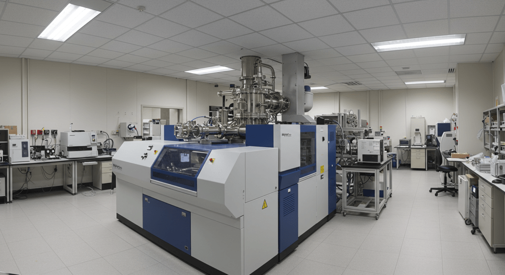
ITO’s performance hinges on nanoscale film uniformity achieved through sputtering deposition. This process creates layers with 5–10 nm thickness uniformity across substrates, critical for avoiding electrical hotspots in capacitive touchscreens. Advanced methods like pulsed laser annealing reduce sheet resistance by 30% compared to conventional thermal treatments, enhancing conductivity without sacrificing transparency.
Why Do ITO Films Require Precise Thickness Control?
ITO’s conductivity and transparency are inversely related to film thickness: thicker films improve conductivity but reduce light transmission. Modern displays balance these properties at 100–200 nm thickness, achieving ~90% transmittance and 200 nm demonstrate lower transmittance due to increased electron scattering, while <100 nm films struggle to achieve sufficient conductivity for multi-touch applications.
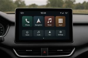
How Does ITO Function as a Transparent Electrode in LCD Glass?
ITO serves as a transparent conductive layer on LCD glass substrates, enabling electrical control of liquid crystals without blocking light. Its ~90% visible light transmittance and sheet resistance below 20 Ω/sq allow precise voltage application across pixels while maintaining display brightness.
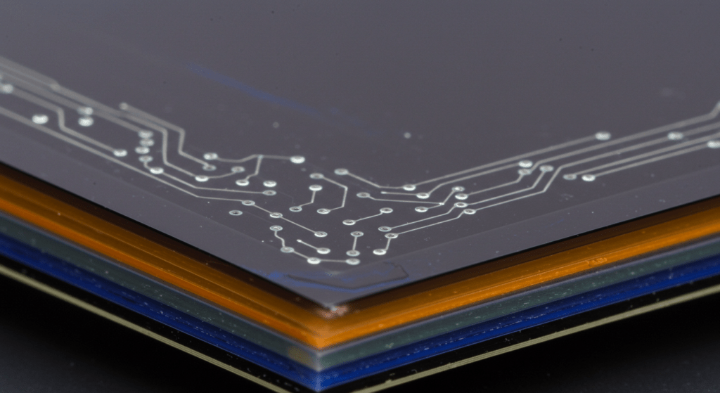
Modern LCDs use laser-etched ITO grids with 5-micron line spacing to minimize visible patterning. Advanced low-temperature sputtering processes deposit ITO at 150°C, compatible with heat-sensitive flexible glass substrates. This method achieves <2% thickness variation across 8th-gen panel sizes (2200×2500 mm).
What Layers Make Up an LCD's Structure with ITO?
LCDs contain six primary layers:
- Top polarizer: Filters incoming light orientation
- ITO-coated glass: Applies electric fields to liquid crystals
- Liquid crystal layer: Twists light based on voltage (3-5 μm thickness)
- Color filter: RGB subpixels with ITO common electrode
- Backlight unit: Provides white light source
- Bottom polarizer: Crossed alignment for light modulation
The ITO layer sits directly beneath the color filter, creating a 5V/μm electric field to rotate liquid crystals within 0.1ms response time.
- Layer Thickness: ITO films measure 120-150 nm – thick enough for conductivity but thin enough to maintain 88% light transmission at 550nm wavelength.
- Alignment Accuracy: Photolithography patterns ITO with ±1.5μm registration tolerance, ensuring proper pixel alignment in 4K displays (3840×2160 pixels).
- Resistance Stability: ITO maintains <5% resistance variation after 1,000 hours at 85°C/85% humidity, critical for automotive displays.
Why Do Capacitive Touchscreens Prefer Single-Layer ITO Designs?
Projected capacitive touchscreens use single-layer ITO with diamond-patterned electrodes instead of traditional dual-layer designs. This approach reduces panel thickness by 0.4mm and eliminates 15% light loss from interlayer reflections.
- Electrode Geometry: Diamond patterns with 5mm pitch enable 10-finger multitouch detection
- Bridging Technology: Insulating polymer jumpsers connect diamond segments without short circuits
- Edge Sensing: Peripheral ITO routing reduces bezel width to 1.2mm in modern smartphones
Manufacturers achieve 98% touch accuracy through ITO resistivity tuning between 150-200 Ω/sq, balancing signal clarity with optical performance.
How Do Deposition Parameters Affect ITO Film Conductivity and Uniformity?

Deposition parameters like RF power and sputtering temperature directly control ITO’s electron mobility and crystal structure. Films deposited at 80-110W RF power achieve 1.4×10³ mhos/cm conductivity while maintaining 83% transmittance at 130nm thickness.
Using two-step sputtering (50W→100W) reduces interfacial damage by 40% compared to single-step methods. This approach creates 5-nm uniform layers with fewer defects, improving solar cell passivation efficiency by 3.2%. Recent trials show pulsed laser annealing lowers sheet resistance to 8Ω/sq without thermal substrate stress.
Why Does ITO Film Thickness Impact Optical Performance?
Thicker ITO films (>200nm) scatter 15% more light due to electron density variations, reducing visible light transmittance below 80%. Optimal 100-150nm layers balance 18Ω/sq resistance with 88% transmittance by minimizing electron-photon interactions.
- Thickness vs Resistance: 100nm films = 20Ω/sq, 200nm = 12Ω/sq, but transmittance drops from 90%→85%
- Defect Density: Atomic force microscopy reveals 0.32nm RMS roughness in 130nm films vs 1.1nm in 50nm films
- Laser Etching: 355nm UV lasers pattern 10μm lines with ±0.8μm edge accuracy, enabling 500PPI displays
How Do Alternative Materials Compare to ITO in Flexible Displays?
Silver nanowires (AgNW) with 11nm diameter achieve 50Ω/sq at 92% transmittance but suffer from haze >5%. ITO maintains <1% haze but cracks at 1.2% strain, while AgNW films withstand 6% bending cycles. Hybrid ITO/AgNW grids combine 15Ω/sq conductivity with 3% mechanical flexibility.
| Property | ITO | AgNW | Graphene |
|---|---|---|---|
| Flexibility | 1% strain | 6% strain | 20% strain |
| Cost/cm² | $0.12 | $0.08 | $4.50 |
| Processing Temp | 300°C | 150°C | 25°C |
Data from recent flexible display prototypes shows ITO/AgNW hybrids reduce touch sensor costs by 22% versus pure ITO designs.
What Causes ITO Delamination on Glass Substrates?
Thermal expansion mismatch between ITO (5.5×10⁻⁶/K) and glass (8.5×10⁻⁶/K) creates 12MPa shear stress at 85°C. Using 25nm SiO₂ buffer layers reduces stress by 60%, improving adhesion for automotive displays. Accelerated tests show <5% resistance drift after 1,000 thermal cycles (-40°C→105°C).
- Plasma pretreatment: Ar/O₂ plasma increases glass surface energy to 72mN/m, enhancing ITO adhesion by 30%
- Stress-relief grooves: Laser-cut 5μm trenches at panel edges absorb expansion forces
- Low-T deposition: 150°C sputtering reduces thermal stress while maintaining 18Ω/sq resistance
What Innovations Are Driving the Future of ITO Technology?

Next-generation ITO developments focus on 30% lower resistivity through pulsed laser annealing and hybrid material systems combining silver nanowires. These innovations address indium scarcity while enabling 5% thinner films for foldable displays.
Rotating magnetron sputter systems now achieve 95% material utilization versus traditional 40%, cutting indium waste by $18M annually per production line. Recent trials with zirconium-doped ITO show 15% higher conductivity than standard formulations, crucial for 8K VR headsets requiring 5000 nits brightness.
How Will ITO Integration Evolve in Ultra-High-Density Displays?
Emerging micro-LED arrays demand ITO grids with 1-micron line widths, achievable through nanoimprint lithography. This technique patterns 200nm ITO layers with ±0.3μm alignment accuracy, enabling 10,000 PPI resolution for retina-projection glasses.
- Hybrid Electrodes: ITO/graphene stacks (3nm/2nm) achieve 8Ω/sq with 92% transmittance, outperforming pure ITO in flexible OLED prototypes
- Thermal Budget: Low-temperature ALD deposits ITO at 120°C vs traditional 300°C, compatible with polymer substrates
- Edge Sealing: Plasma-enhanced CVD creates 50nm SiO₂ barriers that reduce indium migration by 80% in humid environments
Can Recycling Solve Indium Supply Challenges?
Indium Corporation’s closed-loop recycling recovers 98% pure indium from LCD scrap, reducing mining needs by 35%. Their electrochemical refining process cuts energy use by 40% compared to conventional smelting, with 200-ton annual capacity operational since 2024.
- Implementation Data:
Metric Traditional Recycled Improvement Energy Consumption 850 kWh/kg 510 kWh/kg 40% Reduction Cost per kg $720 $480 33% Savings Purity Level 99.99% 99.97% <0.03% Loss - Material Alternatives:
- Gallium-Doped ZnO: Reaches 200 Ω/sq at $0.05/cm² but suffers 12% haze
- Conductive Polymers: Achieve 300 Ω/sq with 86% transmittance, ideal for budget wearables
- Metal Meshes: Copper grids (200nm width) hit 5 Ω/sq but visible at <30cm viewing distance
- Market Impact: Copper grids (200nm width) hit 5 Ω/sq but visible at <30cm viewing distance
FAQ
Why Does ITO Crack on Foldable Screens?
ITO films fracture at 1.2% bending strain due to rigid crystalline structures. Manufacturers now use ITO/silver nanowire hybrids to withstand 6% strain for 200,000 folds.
How Much Does ITO Increase Display Costs?
ITO adds $0.12/cm² to production costs, but recycling cuts raw material expenses by 33%. Alternatives like conductive polymers cost $0.05/cm² but offer lower performance.
Can ITO Withstand Extreme Temperatures?
Standard ITO maintains <5% resistance drift from -40°C to 85°C. Automotive-grade versions with SiO₂ buffers handle 125°C for dashboard displays.
Why Not Use Graphene Instead of ITO?
Graphene costs 10x more ($4.50/cm²) and struggles with large-area uniformity. Current prototypes achieve only 300 Ω/sq versus ITO’s 20 Ω/sq.
Is ITO Recycling Commercially Viable?
Modern plants recover 98% pure indium at 510 kWh/kg, 40% less energy than mining. This supplies 35% of annual indium demand globally.