A serial‑in, parallel‑out shift register, like the 74HC595, lets you control many LCD data lines with just a few MCU pins(Parallel vs Serial: Understanding Communication Methods). This setup reduces wiring and makes PCB design easier, especially for displays with wide data buses. Using a SIPO shift register or an integrated serial‑to‑parallel converter helps solve I/O limitations on most microcontrollers. This method improves signal integrity and allows you to use SPI or bit‑banging firmware to update the display quickly and reliably. The approach supports modular LCD systems, including embedded, SPI LCD, or LVDS LCD designs. This article explains when and how to use these techniques for simple and high‑performance LCD modules.
Why Is Parallel‑to‑Serial Conversion Necessary for LCD Modules?

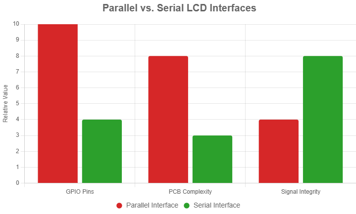
Parallel‑to‑serial conversion is needed because most microcontrollers do not have enough GPIO pins to support a full 8‑ or 16‑bit parallel LCD bus(What is the difference between using an LCD in 4-bit mode versus 8-bit mode when interfacing?). When you use serial data transfer, you can control LCD modules with far fewer pins. This method also makes it much easier to design your PCB and reduces wiring complexity. Fewer signal lines mean it is easier to keep signals stable and reliable, especially over longer cables or in noisy environments(How is CAN or LIN Bus Integration Handled with LCD Modules?).
In real embedded LCD projects, using a parallel LCD interface often means you must allocate at least 8 to 16 dedicated GPIO pins just for data. Many modern microcontrollers only have a few available pins after accounting for other peripherals. This leads to tough choices during design. Using a serial interface like SPI LCD or LVDS LCD allows teams to use only three to five wires for display control(What is an LCD controller board?). This approach not only saves physical space on the PCB but also makes cable assembly simpler and lowers manufacturing costs. In several projects, switching to a serial to parallel converter or a shift register IC helped overcome both space and signal noise issues, leading to faster development and fewer layout revisions(Exploring LVDS and MIPI Interface).
| Feature | Parallel Interface | Serial Interface |
|---|---|---|
| Required GPIO Pins | 8-16 | 3-5 |
| PCB Complexity | High | Low |
| Wiring Count | Many | Few |
| Signal Integrity | Harder (noise, crosstalk) | Easier (fewer lines) |
| Cable Length Handling | Shorter preferred | Longer possible |
| Typical Use | Simple/older LCD modules | Modern/embedded LCDs |
How Does I/O Limitation Affect LCD Interfacing?
I/O limitation affects LCD interfacing by reducing the pins available for other tasks. Parallel LCDs need 8 to 16 pins for data, plus extras for control. Most microcontrollers can’t spare that many GPIO pins. This makes it hard to add sensors, buttons, or other features. In a project I did, connecting a parallel LCD left almost no pins for anything else, forcing a rethink.
A fix is to use serial conversion. I’ve used shift registers to turn parallel data into serial with just three pins. It’s a cheap way to save space. The downside is a small delay from the conversion, but it’s rarely a problem. For example, in a display setup with multiple components, this trick kept everything running smoothly.
Here’s a simple table to compare:
| Type | Pins Used | Good For | Trade-Off |
|---|---|---|---|
| Parallel | 8-16+ | Fast data | Takes lots of pins |
| Serial | 2-4 | Pin savings | Bit slower |
Shift Registers
Shift registers are fundamental components in digital electronics, widely used for data manipulation and transfer. This section dives into their types, internal workings, timing requirements, and key signals, providing a comprehensive understanding of their role in systems like LCD interfaces.
Shift-Register Types & Theory
SIPO (Serial-In, Parallel-Out) vs PISO vs PIPO
Shift registers come in three main types, each defined by how data enters and exits:
- SIPO (Serial-In, Parallel-Out):
Data enters serially (one bit at a time) and is output in parallel (all bits at once). This type is ideal for applications like LCD interfaces, where a microcontroller sends serial data that must be converted to parallel form to drive multiple display pins. For example, a SIPO shift register can reduce pin usage from 16 to just 3 in a 16-bit LCD setup. - PISO (Parallel-In, Serial-Out):
Data is loaded in parallel (all bits simultaneously) and shifted out serially. This is useful for reading multiple inputs (e.g., a keypad) and sending them over a single line to a processor. - PIPO (Parallel-In, Parallel-Out):
Data enters and exits in parallel, typically used for temporary storage or to introduce delays in data processing. It’s less common in interfacing but valuable in specific digital designs.
Each type serves distinct purposes, with SIPO being the most relevant for output-heavy applications like displays.
D-Flip-Flop Chains, Edge-Triggered Clocking
Shift registers operate using a chain of D-flip-flops, where each flip-flop holds one bit of data. Here’s how it works:
- D-Flip-Flop Chains:
Each D-flip-flop’s output connects to the next one’s input, forming a chain. When a clock pulse arrives, data shifts from one flip-flop to the next, moving the entire sequence one position. In a SIPO register, the final outputs are taken in parallel from all flip-flops. - Edge-Triggered Clocking:
Data shifting occurs on the rising or falling edge of the clock signal (depending on the design). This ensures precise timing—data is only captured when the clock transitions, preventing glitches. For instance, in a 4-bit SIPO register, four clock pulses shift in a complete data word, which is then latched to the outputs.
This mechanism is efficient and reliable, making shift registers a staple in digital systems.
Clock Phase, Setup/Hold Requirements
Timing is critical for shift register operation. Key parameters include:
- Clock Phase:
Determines whether data is sampled on the rising edge (e.g., 0V to 5V) or falling edge (5V to 0V) of the clock signal. This must match the register’s specification. - Setup Time:
The minimum time data must be stable before the clock edge. If data changes too late, it may not be captured correctly. - Hold Time:
The minimum time data must remain stable after the clock edge. Premature changes can corrupt the stored value.
A simple timing diagram illustrates this:
					Clock:    ____|----|____|----|____
Data:     -----[Bit1]-----[Bit2]---
Setup:    |<-->|
Hold:           |<-->|
Key Signals
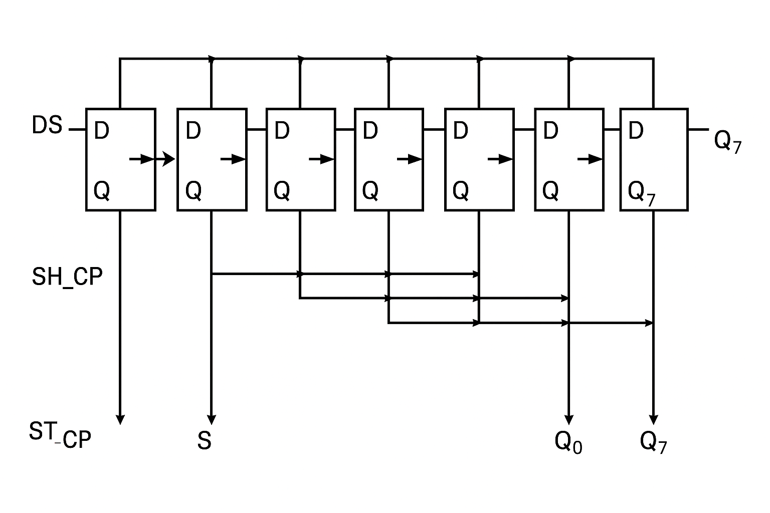
Shift registers rely on specific signals to control their operation. Here’s a breakdown:
- DS (Data Serial):
The input pin where serial data enters the register. Each clock pulse shifts this data into the first flip-flop, pushing existing data forward. - SH_CP (Shift Clock):
The clock signal that drives data shifting. Each pulse (rising or falling edge, per the design) moves data one position through the flip-flop chain. For a 4-bit register, four pulses load a full word. - ST_CP (Latch Clock):
Transfers the shifted data to the parallel outputs. After all bits are in place, a pulse on ST_CP updates the output pins simultaneously, ensuring the LCD receives a complete, synchronized data word. - OE (Output Enable):
Controls the output state. When active (e.g., low), outputs are enabled; when inactive (e.g., high), outputs are disabled (often high-impedance). This is useful for multiplexing or power management.
Here’s a summary table:
| Signal | Function | Role in Operation |
|---|---|---|
| DS | Serial data input | Feeds data into the chain |
| SH_CP | Shift clock | Shifts data bit by bit |
| ST_CP | Latch clock | Updates parallel outputs |
| OE | Output enable | Enables/disables outputs |
Why Shift Registers Matter
Shift registers simplify data handling in constrained systems. In LCD interfaces, a SIPO register can drastically reduce pin requirements, making designs cleaner and more efficient. However, success hinges on understanding their types, internal mechanics, timing needs, and signal roles—mastering these ensures reliable performance in real-world applications.
How Do You Wire and Cascade 74HC595 Shift Registers for LCDs?
The 74HC595 shift register is a powerful tool for LCD interfacing, converting serial data from a microcontroller into parallel outputs for the LCD. This section explains how to wire a single 74HC595 to an LCD and microcontroller, and how to cascade multiple registers to handle larger data needs, such as 16-bit or 24-bit LCDs. This approach minimizes pin usage and offers scalability for embedded projects.
How Do You Wire a 74HC595 to an LCD and Microcontroller?
To connect a 74HC595 to an LCD and a microcontroller (MCU), you need to link specific pins for data transfer and control. Here’s the wiring setup:
- DS (Data Serial): Connect to an MCU GPIO pin. This is the serial data input.
- SH_CP (Shift Clock): Connect to another MCU GPIO pin. This shifts data into the register.
- ST_CP (Latch Clock): Connect to a third MCU GPIO pin. This updates the parallel outputs.
- OE (Output Enable): Connect to ground (GND) to keep outputs always enabled.
- Q0–Q7 (Outputs): Connect to the LCD’s data lines (e.g., D0–D7 for an 8-bit LCD).
- LCD RS and E pins: Connect directly to MCU GPIO pins for register select and enable signals.
This configuration lets the MCU send serial data to the 74HC595, which then drives the LCD’s parallel data lines. Grounding OE ensures the outputs are always active, simplifying operation.
Wiring Table
| 74HC595 Pin | Connect To |
|---|---|
| DS | MCU GPIO (data) |
| SH_CP | MCU GPIO (shift clock) |
| ST_CP | MCU GPIO (latch clock) |
| OE | GND |
| Q0–Q7 | LCD D0–D7 |
| LCD RS, E | MCU GPIOs |
How Do You Cascade Multiple 74HC595 Registers for Larger LCDs?
For LCDs requiring more than 8 bits (e.g., 16-bit or 24-bit displays), you can cascade multiple 74HC595 registers. Here’s how:
- Chaining: Connect the Q7’ (serial output) of the first register to the DS of the next register. Data shifts through the chain sequentially.
- Shared Clock and Latch Lines: Connect SH_CP and ST_CP of all registers to the same MCU GPIO pins. This synchronizes data shifting and latching across all registers(How Do You Calculate the Dot Clock for an LCD Display?).
- Data Transmission: Send the full data word serially. For two registers (16 bits), the first 8 bits shift into the second register, and the last 8 bits stay in the first. For three registers (24 bits), the process extends accordingly.
- Output Update: A single ST_CP pulse updates all register outputs simultaneously, delivering the complete data word to the LCD.
Example: 16-Bit Setup
- First Register: DS from MCU, Q7’ to second register’s DS, Q0–Q7 to LCD D0–D7.
- Second Register: DS from first register’s Q7’, Q0–Q7 to LCD D8–D15.
- Shared Lines: SH_CP and ST_CP from MCU to both registers.
Send 16 bits serially, then pulse ST_CP to display all 16 bits at once. This method scales easily—add more registers for 24 bits or beyond, connecting each Q7’ to the next DS.
Key Benefits
- Reduces MCU pin usage significantly.
- Supports larger LCDs without complex wiring.
- Maintains timing simplicity with shared clock signals.
How Do You Implement Firmware for Shift Register Control in LCD Interfaces?
Implementing firmware for shift register control in LCD interfaces involves selecting the right method to send data from the microcontroller to the shift register. The two primary methods are bit-banging and using the SPI peripheral. Additionally, performance can be optimized with techniques like DMA and interrupt-driven buffering.
What Is Bit-Banging and How Do You Use It for Shift Registers?
Bit-banging is a software technique where the microcontroller manually controls the pins to simulate a serial interface. For shift registers in LCD interfaces, this involves setting the data pin (DS) for each bit and pulsing the shift clock (SH_CP), followed by latching the data with ST_CP and enabling the LCD with the E pin.
In practice, bit-banging requires a loop that processes each bit individually. While it is flexible in terms of pin usage, it can be slower and more CPU-intensive than hardware-based methods. This makes it best suited for applications where timing is not critical or when specific pin assignments are necessary.
What Are the Best Practices for Optimizing Shift Register Performance?
To optimize performance in shift register control, use hardware SPI for faster data transfer, leverage DMA for automated data handling, and implement interrupt-driven buffering for smooth operation at high refresh rates.
- Use Hardware SPI: Faster and more efficient than bit-banging.
- Implement DMA: Automates data transfers, reducing CPU load.
- Use Interrupt-Driven Buffering: Ensures timely data updates without blocking the main program.
While these optimizations can significantly improve performance, they also increase complexity. For many projects, standard SPI without DMA or interrupts is sufficient. Choose the level of optimization based on your project’s specific needs.
What Are the Main Alternative Methods for Serial‑to‑Parallel LCD Conversion?
There are several alternative ways to achieve serial-to-parallel conversion for LCD control. You can use I²C or SPI port expanders to add extra outputs with only two or three wires. Another option is a UART-to-parallel bridge IC, which uses a standard serial port to drive parallel LCDs. For faster and easier code, some LCD modules come with a built-in serial interface like SPI or I²C, though this often costs more. The most flexible approach is an FPGA, which lets you create any timing or protocol you need, but is only practical for complex or high-speed display tasks(How to Implement UART for Monochrome LCD Communication?).
In real embedded projects, the I²C port expander (like PCF8574) makes it easy to add many output lines with only a two-wire bus. However, the protocol overhead of I²C means slower refresh for large LCDs. Using an SPI port expander speeds up data but increases wiring slightly. Some teams prefer UART-to-parallel bridge ICs to offload the bit conversion from the MCU, but you need a free UART and may have lower throughput. Many modern modules come with their own built-in SPI or I²C interface, so you only send simple commands, making code much easier. When displays need custom refresh rates or non-standard signals, some engineers choose FPGAs, but this takes more time and raises cost, so it’s usually reserved for high-performance or special use cases.
| Method | Wiring | MCU Resources | Speed | Cost | Complexity | Typical Use Case |
|---|---|---|---|---|---|---|
| I²C Port Expander | 2 wires | I²C | Moderate | Low | Low | Simple control, low speed LCDs |
| SPI Port Expander | 3 wires | SPI | High | Moderate | Low | Higher speed, more outputs |
| UART‑to‑Parallel IC | 2 wires | UART | Moderate | Moderate | Low-Med | Serial LCDs with UART MCU |
| Serial LCD Module | 2/3 wires | SPI/I²C | High | High | Very low | Easy code, compact projects |
| FPGA Solution | Custom | Any | Highest | Highest | High | Advanced, custom timing needed |
What Design Factors Affect Serial‑to‑Parallel LCD Systems?
Advanced design factors for serial‑to‑parallel LCD control focus on signal integrity, reliability, and component cost. Long cable runs or high-speed signals often need buffer or driver chips to maintain data quality. Proper PCB layout, termination, and decoupling help avoid signal loss or interference. Sequencing the latch-enable signals correctly and adding checks like checksums or CRC can make the system more reliable. When choosing parts, compare low-voltage shift registers like 74HC595 with high-voltage drivers such as HV5622. Always check if key modules are available for your BOM to avoid project delays.
In practical designs, buffer chips are often used when the distance from MCU to LCD is long, preventing signal degradation. Good termination at the ends of long lines and careful decoupling with capacitors near ICs can prevent glitches and noise. During firmware updates, teams have seen fewer display errors when latch-enable sequencing is handled in strict order. Some systems add a simple checksum or even a CRC to the data before latching, which allows for error detection and safer updates. When evaluating shift registers, the 74HC595 is affordable and widely available, but for larger displays or higher voltages, engineers sometimes choose HV5622 at a higher cost. It’s important to check component lead times and stock levels when finalizing the BOM, as sourcing delays can affect production.
| Parameter | 74HC595 | HV5622 |
|---|---|---|
| Voltage range | 2–6V | Up to 80V |
| Max outputs | 8 | 32 |
| Cost | Low | Higher |
| Availability | Wide | Limited |
| Application | Standard LCD | High-voltage LCD |
Related Articles:
Are all common character LCD modules based on the Hitachi HD44780 controller?
How Do Phase-Locked Loops Synchronize Timing in LCD Systems?
How can I reduce LCD power consumption in embedded systems?
How is CAN or LIN Bus Integration Handled with LCD Modules?
What Causes Crosstalk in LCDs and Why Do Active Matrix LCDs Perform Better?
FAQ
What is the impact of using a shift register on update latency?
Using a SIPO shift register adds only a few microseconds per byte for clock and latch cycles, which is negligible compared to full-screen refresh times.
How can I minimize power draw when driving an LCD via shift registers?
Lower the clock frequency and disable unused outputs via the OE pin to cut dynamic and static power consumption.
What common wiring errors cause display glitches?
Tying OE incorrectly or swapping SH_CP and ST_CP lines often leads to flicker or no output, so double‑check pin mappings on both MCU and shift register.
Can I interface multiple voltage domains with a 74HC595?
Yes, use level‑shifters on data and clock lines or choose a version of the IC rated for your MCU’s and LCD’s voltage levels.
What Happens If Shift Register Clock Signals Are Misaligned?
Misaligned clock signals cause data corruption in shift register ICs. Ensure SH_CP and ST_CP timing matches the datasheet to avoid errors.