Some LCD modules need a negative voltage on the VEE pin to set the liquid crystal cell at a mid bias. This split lets the display use a wider voltage swing for dark and bright states and yields sharper visuals(What Are the Differences Between VCC, VDD, VSS, and VEE in LCD Power Inputs?).
The negative offset shifts the operating point into a steeper part of the voltage–contrast curve. This change boosts the light modulation per volt and makes the display more readable(How to Troubleshoot and Test Your Monochrome LCD Module).
Why Does Negative Bias Improve LCD Contrast?

Applying negative bias to an LCD changes the way liquid crystal cell voltage controls the alignment of molecules. When the circuit uses a negative bias, the LCD can move liquid crystals more completely between the black state and the white state. This stronger control lets the display produce a higher contrast ratio. Negative bias also helps balance the overall voltage applied to the panel, which reduces DC biasing. This protection stops ionic migration inside the screen, helping the LCD show deep blacks and bright whites for a long time. Negative bias keeps the electro-optical response stable and avoids image retention. These changes give the display a clear advantage in display longevity and day-to-day viewing().
Engineers in practical projects find that using negative bias keeps the alignment of liquid crystals more precise. When the drive circuit uses negative and positive voltages in turn, the display voltage across the cell returns to zero on average. This stops slow damage that would happen if the LCD had a constant positive voltage. Real project tests show that screens with negative bias show fewer artifacts and keep a strong contrast ratio over thousands of hours. Using negative bias also keeps the voltage threshold steady, so the black state and white state do not shift as the screen ages. This means images stay clear, and the screen resists ghosting(What Does Contrast Ratio Mean on a Monitor?).
Key Effects of Negative Bias on LCD Contrast:
- Negative bias lets liquid crystals move quickly and fully between states
- Increases and stabilizes contrast ratio in every use
- Stops ionic migration and protects cell structure
- Keeps the black state deep and uniform in all conditions
- Reduces image retention and slows visible wear
- Controls DC biasing so the panel voltage stays balanced
- Gives longer display longevity with strong, steady performance
- Holds a steady electro-optical response under many signal types
- Keeps the white state bright and clear, without extra voltage
How Does Liquid-crystal Cell Voltage Relate to Contrast?
The liquid crystal cell voltage controls how the molecules twist inside the LCD. When the voltage is low, the molecules block light and create the black state. When the voltage rises above a key voltage threshold, the molecules untwist and let more light pass, forming the white state. The difference between these two states is the contrast ratio. If the voltage is not right, the LCD can look gray or washed out. Stable cell voltage is needed for high LCD contrast.
In practical work, engineers set the drive voltage to make sure every pixel can fully change between black and white. They watch for display voltage drift, which can lower contrast and make images look weak. Engineers use precise circuits to adjust voltage, so the LCD keeps sharp images and strong contrast in any light. If voltage is too low, the black state is weak and some pixels may not fully turn off. If voltage is unstable, users may see ghosting or flickering. Good voltage control gives the LCD both clear images and long display longevity.
How Cell Voltage Affects LCD Contrast (Quick Points):
- Liquid crystal cell voltage sets crystal twist for each pixel
- Need to pass a voltage threshold for full white state
- Low voltage causes weak black state
- Display voltage drift leads to gray or unclear images
- Tight voltage control keeps contrast ratio high
- Good voltage prevents ghosting and brightness problems
- Stable voltage keeps display longevity
- Strong contrast in both bright and dark places
What Is the Difference Between Positive-only and Bipolar Drive Waveforms?
A positive-only drive waveform uses only positive voltages across the LCD cell, while a bipolar drive waveform switches the voltage from positive to negative in each cycle. The bipolar drive balances the total voltage over time, which keeps the average voltage near zero. This balancing prevents DC biasing and ionic migration that can damage the display. The bipolar waveform also helps maintain a stable contrast ratio and reduces the risk of image retention(What is a Bistable Display and How Does It Work?).
In field projects, engineers see that displays using positive-only drive can show slow drops in LCD contrast and more frequent ghosting over long periods. These problems come from ions moving inside the liquid crystal layer and building up at the electrodes. Bipolar waveforms, by changing polarity, stop this buildup and let the display keep deep blacks and clear whites. Circuits that use bipolar drive are now standard in most new designs to keep screens looking sharp in daily use and extend display longevity.
Comparison: Positive-only vs. Bipolar Drive (Key Points):
| Drive Method | Key Features | Main Issues |
|---|---|---|
| Positive-only | Uses only positive voltage, simple control | Builds up DC biasing, leads to ionic migration, weaker contrast ratio over time |
| Bipolar | Alternates positive and negative voltages, balances cell voltage | Prevents DC biasing, keeps contrast ratio steady, extends display longevity |
What Are VO and VEE Pins and How Are Their Voltage Ranges Used?
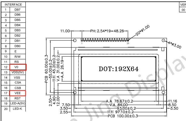
The VO pin and VEE pin are used on many LCD modules to set and supply the LCD contrast voltage. The VO pin often serves as the reference voltage for contrast adjustment, while the VEE pin supplies a stable negative voltage needed by the LCD panel’s internal circuits. Setting the right voltage at these pins decides how the liquid crystals twist, changing the screen’s appearance from dark to bright. If the voltage is too high or too low, the contrast adjustment will not work well, and the display may look faded or unreadable. Engineers use these pins to set the best balance between black state and white state for a clear image(Embedded Development Basic Tutorial: Detailed Explanation of the 16×2 LCD Module).
In project work, the VO pin is usually connected to a voltage divider or a potentiometer control so users can adjust contrast directly. The VEE pin may come from an internal or external negative voltage generation circuit. Designers check the datasheet interpretation to make sure voltages stay within the safe voltage range (often –2 V…–8 V typical). If the voltage goes outside this range, it can cause image issues or even damage the display. Setting up the power supply for these pins is one of the first steps in LCD drive circuit design.
Key Points for VO/VEE Pin and Voltage Ranges:
- VO pin is the main contrast voltage input
- VEE pin supplies stable negative voltage for biasing
- Both affect LCD contrast voltage directly
- Incorrect voltages can damage the LCD
- Check the datasheet interpretation for recommended ranges
- Use a potentiometer or voltage divider to adjust VO pin
- Negative voltage generation may be internal or external
- Proper pinout and connection are needed for safe setup
- Stable voltages give best contrast adjustment and long life
- Keep all voltages inside safe voltage range (e.g., –2 V…–8 V)
How Should Datasheet Voltage Ranges Like –2 V…–8 V Be Understood?

Datasheet voltage ranges such as –2 V…–8 V show the typical limits where the LCD contrast voltage can be safely set. The lower number is the minimum voltage needed to start seeing changes in contrast adjustment. The upper number is the maximum voltage before the display starts to show distortion or risk damage. These numbers guide engineers in picking power supply levels and in designing voltage control circuits. Staying inside this range lets the bias voltage set the screen’s darkest and brightest states without stressing the liquid crystal layer(How is the Color Filter Layer Created in LCD Panels?).
In practice, engineers use a multimeter to check voltages at the pins during setup and adjustment. The VO pin is often adjusted up or down within the datasheet range until the best image is found. If the voltage drops below –2 V, the LCD may lose contrast; if it goes above –8 V, ghosting or permanent spots can appear. These numbers are typical, but each LCD model may have slightly different limits, so it is always needed to read the correct datasheet for each part. Project experience shows that keeping voltages stable inside the recommended range avoids both short-term image issues and long-term aging effects.
VO/VEE Voltage Range Reference Table:
| Parameter | Typical Range |
|---|---|
| VO pin voltage | –2 V…–8 V |
| VEE pin voltage | –2 V…–8 V |
| Multi-stage bias | Varies by circuit |
What’s the Difference Between VO, VEE, and Multi-stage Bias Pins?
The VO pin is used mainly for contrast adjustment. It usually connects to a simple control like a potentiometer or a digital-to-analog circuit to let the user or controller set the display’s darkness. The VEE pin provides a negative voltage reference, either created inside the LCD module or supplied from outside. This voltage is more stable and is not usually adjusted in normal use. Multi-stage bias pins are used on some advanced LCD panels to split the bias voltage into several steps. This design makes the display more uniform, reduces flicker, and gives better control over contrast voltage at different points across the panel.
In engineering, choosing between a simple VO/VEE setup or a multi-stage bias scheme depends on the project’s needs. For most basic text LCDs, VO and VEE are enough. For high-quality graphics displays, multi-stage bias gives better image quality but is harder to set up. The correct wiring and voltage control are needed for each system. Engineers check the datasheet’s pinout, look at typical voltage levels, and match their power supply design to the right pin functions.
VO vs. VEE vs. Multi-stage Bias (Key Differences):
| Pin Type | Function | How Adjusted | Use Case |
|---|---|---|---|
| VO pin | Main contrast adjustment | Potentiometer/voltage div. | All LCDs, basic/advanced |
| VEE pin | Stable negative reference voltage | Power supply, fixed | Needed for many basic and graphic LCDs |
| Multi-stage bias | Steps bias for even contrast | Multiple taps, resistors | High-end, low-flicker LCDs |
What Are the Main Methods for Generating Negative Voltage?
Negative voltage generation is needed for LCD biasing and many analog circuits. Three main methods are widely used: charge-pump ICs (like ICL7660 and MAX232), op-amp inverter circuits, and discrete transistor charge-pump circuits for hobbyists. Each method has its own wiring needs, parts, and trade-offs in efficiency, output current, and ripple voltage. The best choice depends on available components, circuit complexity, and how much negative current your LCD or circuit requires.
In practical design, engineers pick the charge-pump IC for its easy wiring and small size. For low-current analog needs, an op-amp inverter is simple to add. For hobby and learning, the discrete transistor charge-pump helps users understand circuit basics and build with simple parts. Keeping all methods in mind lets designers choose the right solution for both new designs and quick fixes.
Key Methods and Quick Points:
- Charge-pump IC: Reliable, low parts count, popular for LCD modules
- ICL7660/MAX232: Simple to wire, built-in oscillators, just add caps
- Op-amp inverter: Good for small loads, quick to prototype
- Discrete transistor charge-pump: DIY, easy parts, fun for hobbyists
- Each has different efficiency, output current, and circuit size
| Method | Efficiency | Output Current | Component Count |
|---|---|---|---|
| Charge-pump IC | High (70-95%) | 10–100 mA | Low |
| Op-amp inverter | Moderate | <10 mA | Low |
| Discrete transistor pump | Varies, moderate | 1–20 mA | Moderate |
How Do You Generate Negative Voltage with Charge-pump ICs (ICL7660 / MAX232)?
Charge-pump ICs like ICL7660 and MAX232 make negative voltage from a positive supply using capacitors. They work by rapidly switching the charge between capacitors and inverting the voltage at their output. The most common wiring connects two or more capacitors to the IC pins as shown in the datasheet. Choosing the right cap values (often 1–10 μF ceramic or tantalum) keeps ripple voltage low and supports higher output current. Many LCD modules use these ICs because they are simple and reliable.
When wiring the ICL7660, connect the supply voltage (+5 V) to V+, ground to GND, and connect two 10 μF caps: one from pin 2 to ground, another between pin 2 and pin 4 (CAP+ to CAP–). The output at pin 5 gives you a negative voltage (about –5 V if the input is +5 V). For MAX232, more caps are used for extra internal voltage doublers and inverters, but the wiring is just as easy. In real projects, these ICs power LCD bias lines or op-amp rails where a small, stable negative voltage is needed. They are small, cheap, and need no transformers or coils.
Wiring a Charge-pump IC (ICL7660 Example):
- V+ (Pin 8): Connect to +5 V
- GND (Pin 3): Connect to ground
- CAP+ (Pin 2): Connect to one side of capacitor (10 μF)
- CAP– (Pin 4): Connect to other side of same cap
- VOUT (Pin 5): Negative voltage output (about –5 V)
- Add a 10 μF cap from VOUT to ground
What Are the Pros and Cons of Op-amp Inverter Circuits?
An op-amp inverter circuit uses an op-amp, a few resistors, and often a reference voltage to create a negative output from a positive supply. The op-amp is set up to invert the voltage at its non-inverting input, so the output becomes negative. This approach is best for circuits that need only a small amount of current, like reference rails or sensor biasing. It is very simple to build, but the output current is much lower than charge-pump ICs. The ripple voltage is also usually higher. For most LCD bias needs, it is only good for driving control voltages, not main power rails.
Pros:
- Easy to prototype and test
- Uses standard op-amps found in any lab
- Good for low-current, stable reference voltages
- Can be made adjustable with resistors
Cons:
- Output current is low (<10 mA typical)
- Ripple voltage can be high if load varies
- Efficiency is lower than charge-pump IC
- Not suitable for power-hungry circuits
How Can Hobbyists Build a Discrete Transistor Charge-pump?
A discrete transistor charge-pump is a DIY way to make negative voltage using a few transistors, diodes, and capacitors. It works by using a square wave (from a timer IC like 555 or an MCU pin) to switch current through the network, charging and moving voltage across the caps to generate a negative output. This circuit is simple to build from parts found in old radios or scrap, which is why hobbyists and students use it for LCDs or small sensors.
A classic design uses two NPN transistors, two diodes, and two capacitors. The timing pulse turns the transistors on and off, pumping charge from input to output. Output voltage depends on the input supply, the speed of switching, and the cap size. Output current is usually lower than with ICs, and ripple can be higher, but it works for light loads and is easy to repair or modify. Common mistakes are using too small capacitors or wrong transistor pinouts.
DIY Discrete Charge-pump (Step-by-step):
- Use a square wave (from 555 timer or MCU)
- Connect two NPN transistors (e.g., 2N3904) in charge-pump topology
- Use two diodes (e.g., 1N4148) for steering charge
- Add two electrolytic capacitors (10–47 μF)
- Output taken from diode-capacitor junction as negative voltage
How Do You Design an Effective LCD Contrast Adjustment Circuit?
A reliable LCD contrast adjustment circuit uses a potentiometer to control the voltage between VEE (negative bias) and VSS (GND), feeding this voltage to the LCD’s contrast pin (often VO or V0). This setup acts as a voltage divider, allowing smooth control of the screen’s dark and bright balance. Good design makes adjustment easy, gives a full range of contrast adjustment, and stops noise or supply issues from affecting LCD clarity. Stable resistor values and the right potentiometer size help keep the image clear, while bypass and decoupling capacitors reduce noise and flicker, protecting signal integrity.
In real projects, using a standard value potentiometer (like 10 kΩ or 20 kΩ) between VEE and GND gives most LCDs full contrast control. Placing bypass capacitors (such as 0.1 μF ceramic) near the VEE or VO pin, and adding a larger decoupling capacitor (like 4.7 μF or 10 μF electrolytic) at the supply pin, makes the contrast stable and prevents screen artifacts. Wiring should be short and direct, with clean pinout to avoid parasitic noise. Careful component choice and layout keeps the LCD image crisp under all conditions.
Checklist for Effective LCD Contrast Adjustment:
- Connect potentiometer between VEE and VSS (GND)
- Wiper to VO/V0 pin for variable voltage
- Use 10 kΩ or 20 kΩ pot for smooth control
- Add bypass capacitor (0.1 μF) close to VO/VEE
- Add decoupling capacitor (4.7–10 μF) at power input
- Keep wiring short and avoid loops
- Double check LCD pinout for correct VO/VEE pins
- Test range for full contrast adjustment
- Adjust pot for best LCD clarity
How Do You Use a Potentiometer Between VEE and VSS (GND) for Contrast Control?
A potentiometer acts as an adjustable voltage divider between VEE and VSS (GND). The wiper outputs a variable voltage, which connects to the LCD’s VO (or V0) pin. Turning the pot changes the output voltage, adjusting the electric field inside the display and shifting the contrast adjustment smoothly from minimum (almost white) to maximum (deep black).
To wire it: connect one end of the pot to VEE (usually the most negative voltage), the other end to VSS (GND), and the center wiper to VO. This wiring works for both standard text LCDs and many graphic modules. In many projects, this simple layout lets users tune display readability for different environments. Project experience shows that direct wiring and clean connections make adjustment easy and avoid dead spots or uneven contrast.
Potentiometer Wiring for Contrast Adjustment:
- One pot end to VEE
- Other pot end to VSS (GND)
- Pot wiper to VO/V0 pin
- (Optional) Add a bypass capacitor (0.1 μF) from VO to GND
What Resistor Values and Potentiometer Sizes Are Recommended?
For most LCDs, a potentiometer between 5 kΩ and 20 kΩ gives the smoothest contrast adjustment. The most common value is 10 kΩ. Lower values (1 kΩ–5 kΩ) can work but may drain more current from VEE and sometimes give a less precise adjustment. Higher values (over 20 kΩ) can make the control too sensitive and the contrast harder to set. In fixed-voltage designs, two resistors as a divider (such as 10 kΩ top, 4.7 kΩ bottom) can also be used, but a pot gives better user control(How Do Sunlight-Readable LCDs Maintain Contrast Outdoors?).
Table: Recommended Potentiometer and Resistor Values
| Component | Value Range | Typical Use |
|---|---|---|
| Potentiometer | 5 kΩ – 20 kΩ | Adjustable contrast |
| Potentiometer | 10 kΩ | Most common LCD use |
| Fixed resistor | 10 kΩ / 4.7 kΩ | Simple divider, no user control |
Project tip: Choose a pot with a smooth rotation and linear (B) taper. Wire as close as possible to the LCD to reduce parasitic noise.
How Do Bypass and Decoupling Capacitors Suppress Noise?
Bypass capacitors (like 0.1 μF ceramics) and decoupling capacitors (like 4.7 μF or 10 μF electrolytics) are key to noise suppression and supply stability in LCD contrast circuits. Placed close to the VO, VEE, and power supply pins, they shunt high-frequency noise and filter voltage dips caused by fast switching or nearby digital circuits. This keeps the signal integrity of the contrast voltage, avoids flicker, and gives steady, clear images.
In field work, even small bursts of digital noise or supply ripple can make an LCD show lines, flicker, or lose LCD clarity. Using at least one bypass cap near the VO/VEE pins blocks most noise. Adding a bigger decoupling cap at the power supply further filters low-frequency hum and keeps the contrast stable during fast changes.
Where to Place Bypass and Decoupling Capacitors:
- Bypass capacitor (0.1 μF): as close as possible to VO/VEE
- Decoupling capacitor (4.7–10 μF): near main LCD supply pin
- Keep leads short for best filtering
- Place both caps on same PCB side as LCD
Why Is Power Sequencing Important for LCDs?
Power sequencing is critical for LCDs because it ensures the positive supply voltage (VDD) is applied before the negative supply voltage (VEE). This order prevents damage to the LCD driver circuitry and ensures the display operates correctly. In LCD systems, VDD powers the logic and control sections, while VEE provides the negative voltage needed for contrast. Applying VEE before VDD can expose the driver ICs to negative voltages without a stable positive supply, risking issues like latch-up or permanent damage.
Imagine starting a car: you turn the key (VDD) before pressing the gas pedal (VEE). If you skip the key and mash the gas, the car might not start—or worse, it could break. Similarly, incorrect sequencing in an LCD can lead to malfunctions or a shorter lifespan.
Here’s what can happen if sequencing goes wrong:
| Sequencing Issue | Potential Problem |
|---|---|
| VEE before VDD | Driver ICs may latch up or fail |
| VDD and VEE at the same time | Uncontrolled voltages on LCD segments |
| VEE removed after VDD | LCD partially powered, risking damage |
Proper sequencing keeps the LCD safe and reliable.
Why Must VDD Precede VEE on Power-Up?
VDD must come before VEE on power-up because the control logic, powered by VDD, needs to be active to manage VEE’s application. Without VDD, the driver ICs can’t control the LCD segments, and applying VEE first could send uncontrolled voltages across the display, potentially damaging it.
In an LCD setup, the control logic dictates how voltage reaches the liquid crystal cells. If VEE kicks in before VDD, it’s like trying to steer a car with no engine power—things go haywire. For instance, VEE without VDD might overvolt the LCD segments, degrading the liquid crystals or frying the driver circuits. To prevent this, ensure VDD stabilizes first, using power management ICs or a circuit design that naturally prioritizes VDD.
How Can You Ensure a Safe Shutdown to Avoid LCD Damage?
For a safe shutdown, remove VEE before VDD. This avoids leaving the LCD with a negative voltage while the control logic is off, which could cause uneven charges or degrade the display over time.
If VDD drops first during shutdown, VEE might linger, keeping the LCD partially powered without oversight from the driver ICs. This can harm the liquid crystals. To fix this, design the circuit to cut VEE before VDD—think of it like parking a car: release the gas (VEE) before turning off the engine (VDD). Use power management chips with built-in sequencing or add a timing circuit, like an RC delay, to drop VEE first. A microcontroller can also handle this by switching off VEE, waiting a moment, then cutting VDD.
What Protection Components Can Be Added to Safeguard the Circuit?
To protect the circuit, add series resistors and protection diodes. Series resistors limit inrush currents during power-up, easing the strain from sudden voltage shifts. Protection diodes cap voltages at safe levels, guarding against spikes or sequencing errors.
For example, a 10Ω resistor on the VDD line can tame current surges, protecting sensitive parts. Protection diodes—say, Schottky diodes on input pins—redirect excess voltage to ground or VDD if VEE misfires early. Here’s a basic setup:
- Series Resistor: 10Ω on VDD.
- Protection Diodes: Schottky diodes from inputs to VDD and ground.
- Bypass Capacitor: 0.1µF across VDD and ground for noise control.
These simple additions bolster your LCD circuit’s resilience.
What Are the Main Digital and Software-based LCD Contrast Control Methods?
Digital and programmable contrast control methods use a DAC-based bias or PWM filtering circuit, or a software-driven adjustment feature inside a modern microcontroller (MCU)(What is an LCD controller board?). These approaches make it possible to adjust LCD bias voltage from code, a user interface, or remote system—without turning a physical potentiometer. The main benefits are automated control, precise step-by-step adjustment, remote or programmable user interface, and easy integration into digital product lines. Project teams choose digital methods for better automation, more precision adjustment, or custom UI needs.
Common setups use a microcontroller with a built-in or external digital-to-analog converter (DAC), or a high-frequency PWM output filtered by an RC filter(How Does PWM Control Backlight Brightness in Modern Displays?). The output becomes a stable analog bias for the LCD’s contrast pin. In advanced MCUs, software directly writes the output value, letting users adjust contrast via menus, buttons, or over the network. Field projects show that software-based contrast adjustment is ideal for modern touchscreens, industrial panels, or any LCD that needs flexible or remote operation.
Key Points for Digital Contrast Control:
- DAC-based bias for programmable analog voltage
- PWM filtering creates smooth DC from MCU output
- Software-driven adjustment through registers or APIs
- Works with any LCD requiring analog bias
- Enables remote, UI, or automated control
- No need for manual potentiometers
- Adjustable at any time, even during runtime
- Allows feedback loop or self-tuning algorithms
| Method | Resolution | Hardware Needs | Best For |
|---|---|---|---|
| DAC-based | 8–12+ bit steps | MCU with DAC or ext. | High precision, industrial, pro UI |
| PWM+RC filter | 6–10 bit steps | MCU w/ PWM, RC filter | Low cost, mid-precision |
| Manual potentiometer | Analog smooth | Potentiometer only | Cost down, basic/simple LCDs |
How Does DAC-based Bias Generation with PWM Filtering Work?
A DAC-based bias system uses a digital-to-analog converter or a filtered PWM output to create a stable voltage for the LCD contrast control. The MCU sets the DAC value or PWM duty cycle in software, making the output voltage programmable. The signal then passes through an RC filter (resistor and capacitor) that smooths out any ripple, giving a clean, low-noise DC voltage for the LCD contrast pin. Tuning the filter’s R and C values controls how quickly the output responds and how much ripple remains.
In projects, teams pick a 10–100 kΩ resistor and 1–10 μF capacitor for the RC filter. The higher the PWM frequency, the easier it is to get smooth DC. The DAC or PWM register value is adjusted by the MCU according to user input, remote commands, or automatic feedback. The setup can be tested by sweeping the DAC or PWM values and watching the LCD contrast change. The circuit is small and reliable, and no manual pot is needed.
DAC/PWM Contrast Control Circuit Steps:
- MCU outputs PWM or sets DAC value
- Signal goes through RC filter (e.g., 47 kΩ + 4.7 μF)
- Filter output connects to LCD contrast pin
- Software sets value for desired display appearance
| Parameter | Typical Value |
|---|---|
| PWM frequency | 1 kHz – 50 kHz |
| RC resistor | 10–100 kΩ |
| RC capacitor | 1–10 μF |
| DAC resolution | 8–12 bits |
Related Articles:
How Does Baud Rate Affect Monochrome LCD Data Transmission?
What Are the Differences Between Built-In and External LCD Controllers?
How Do Rise and Fall Times of the Enable Pin Affect Data and Display Quality in LCD1602 Modules?
How do timing controllers (TCON) synchronize image data in LCDs?
What Are the Differences Between SPI and I2C for LCD Modules?
FAQ
What happens if I connect the LCD contrast pin directly to ground?
Connecting the contrast pin directly to ground usually gives very low contrast or a blank display because the bias voltage is not set in the right range.
Can I use the same negative voltage for multiple LCD modules?
Yes, you can share a negative voltage source across several LCD modules, but each display should still have its own contrast adjustment for best clarity.
Will adjusting the LCD contrast affect display lifetime?
Setting the contrast too high or too low for long periods can stress the liquid crystal layer and may shorten usable screen life or cause ghosting.
How can I tell if my LCD module needs a negative voltage?
Check the module’s datasheet for a VEE or VO pin with a negative voltage range, or look for contrast adjustment recommendations that mention negative bias.
Is it safe to use a switching regulator for LCD negative voltage?
Switching regulators are safe if filtered well, but ripple or noise may cause flicker; always test stability with your actual display and load.